You are the visitor n.
Best view with 1024x768 | ||
You are the visitor n.
Best view with 1024x768 | ||
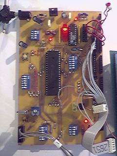
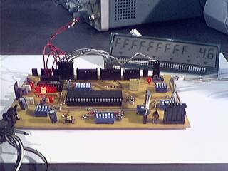 | The Development Board v. 1.1 connected to an LCD display. It is well visible (read further, in the description) the row of LEDs used to check the logic state of up to 8 I/O ports or external circuits' pins. Of course, if you own an 8 trace oscilloscope, you can do without it. :-)) On the right bottom the programming cable. |
| Below, the PCB of the Development Board (version 1.0) - On the right, the DB v. 1.1 at work |
 |  |  |
Back to Home Page | Similar topics on this site: PIC 16F84 F.F. Evaluation Board Connecting a microcontroller to RS-232 ports and PS/2 devices Keypad 4x5 for microcontrollers |
Characteristics of the DB12 As I have done with the PIC 16F84 / C84 Evaluation Board, designed and built by myself according to my need, when approaching a higher level microcontroller I decided to design a circuit allowing easy development of applications. This board, in fact, allows the PIC to be interfaced with external circuits in a reliable and versatile way, making it possible to blame just the external circuits in case of electrical problems, and, of course, to concentrate just on the software. Supported microcontrollers: PIC 16F877, 16F874 Note: the PIC 16F877 pin-out is upwardly compatible with the pin-out of PIC 18F442, 18F452, 18F448, 18F458. This board have been designed for PIC16F877 and tested with it (and on this page we'll always refer to it); the circuit should be anyway suitable for mentioned microcontrollers, too (18F4x2 and 18F4x8), with the following notes: a) the OSC2 pin would be
multiplexed with RA6 Let's now describe the main characteristics of this circuit:
As previously said, this circuit is not a PIC programmer, but
it can be easily interfaced with one of the many programmers you can
find, allowing you not to remove the microcontroller from the board
(in-system programming). NOTE: the images of the layout and the schematics further on this page are at low resolution, for obvious problems concerning the time needed to load this page, but their links point to better resolution images. When you click on a link of an image (i.e. the layout) and a new window opens, I suggest you not to close it, as it could be useful to take a look at it while reading this page and in particular for the examples that are further described. While designing this circuit I tried to realize a versatile
circuit and, in the same time, I also pursued the possibility to mount
only the components one wish, making this D.B. a not expensive one. Images needed to realize the circuit If you wish to realize the Development Board (after reading, in particular, the "Acknowledgement and disclaimers" section), you can find here the links to save the images you need (at 300 dpi), reachable anyway in other points of this page. Advices for printing in the layout printing section further. Copper
side layout at 300 dpi (316 KB) Why so many dip-switches? I have choosen to use a switch for each pin that sometimes has to be insulated or connected to other particular pins (i.e., during programming), both to grant a safe insulation and because using 3-state buffers could not be so easy and they could have some electrical problems (i.e, /RESET and supply). In any case, during the normal switch between use and programming, as an example when the software is being developed, to allow the chip to be programmed it is usually enough to carry out a few simple operations, not more than a few seconds, setting to OFF some switches of a few dip switches and those of another dip-switch to ON (others dip-switches can be left as they are). As soon as the chip is programmed, it is enough to carry out the inverse operation so having the PIC ready again and connected to the external world. In the section "Programming" operations to carry on are reported in details for the various kinds of programmers, their supply and the LVP bit of the PIC. Acknowledgement and disclaimers This project is entirely personal; an acknowledgement goes to
the software allowing me to realize the circuit's layout. It is the
program PCB Elegance v. 2.0; I have it in the FREE version, limited to
200 pins, by MERCO Electronics, which has authorized me by e-mail also
to non-personal purposes. Note: Although it's theoretically possible to use other forms of supply, this Development Board v. 1.2 has been projected to receive supply from 9-12 V batteries and interfaced only with circuits with low voltage batteries supply. There is anyway a 800 mA fuse; see warnings about the fuse on the components' list. In any case, be always aware of what you are doing! Being
this material at free disposal of whoever desires it, it is absolutely
forbidden any form of use for commercial purposes. |
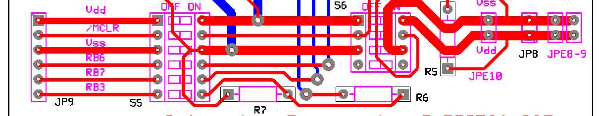
Before going on with the description of of the circuit, let's introduce here a remark. Remark on how to identify switches and connectors' pins References to a particular switch of the dip-switch Sx will be made as Sx-n, the same convention for connectors JPx. The "E" suffix simply means "extra". A reference to the switch Sx-1 points out the first switch of the dip.switch Sx starting counting from top; analogous meaning when referring to connectors. In the image below here, as an instance, S6-4 is not connected to any track; JP9-6 is connected to S5-6, and, when this one is ON, also to R7 and R6.
Another
example in the figure 4 at 200 dpi -
Components placement and tracks layout; the 300 dpi version, printable
with good quality, can be reached at the section layout,
but it requires to be loaded a longer time than the 200 dpi version,
apt to have a look at it. As an example, looking at the image in figure
4, when S5-6 and S3-6 are closed, JP9-6
and the pin number 36 of the PIC (RB3) are connected through R6; when
S5-6 and S3-6 are open, and S3-3 is closed, the RB3 pin is connected
only to JP5-5. Circuit's characteristics and description Let's now go on with the possibilities of this Development Board. If you want, before reading now the description of the various characteristics of this circuit, to have an idea of what this board can allow you to do you could take a look at something practical, that is how to set switches for normal operations . Supply:
the circuit has been projected to be supplied by a 9-12 V battery, but
it is also possible to use an unregulated 7-15 V D.C. source (a 7805
feeds regulated 5V to the PIC, to a possible external circuit and a
possible programmer), or supply from an external circuit through JP8 -
S6 (in this case you must look on Microchip datasheet for the range
allowed). NOTE: the fuse protects only the supply source connected to
J1 (or JPE15); this fuse must be choosen according to the power supply
you are using, and it must have an adequate safety margin (as an
example, for a power supply able to source 500 mA, I advice a fuse
around 250 mA). Beside, also the voltage fed to the 7805 determines the
value of the fuse, as the fuse itself must avoid an excessive power
dissipation in the 7805 (see warnings about the fuse on the components
list). IN ANY CASE, the fuse must not be over 800mA. /MCLR pin:
it is possible to drive it by an external circuit or by a programmer,
to connect it to Vdd directly, or also to Vss through a capacitor to
have a Power On circuit (anyway already present in the PIC); you can
also reset the PIC while working by mean of the switch S4. Connection of Vdd, Vss, /MCLR from and
to the external world: connection from and to
any external circuit of Vdd, Vss, /MCLR (this last one whatever supply
source is being used); connection of Vdd and Vss from or to any
programmer. Clock
source: connector to insert a crystal in
(4MHz, 8 MHz, 12 MHz, 20 MHz tested), RC mode with variable resistor,
for an oscillation regulable over a very wide range (partially tested),
up to a few MHz; Possibility
of leaving the PIC on the Evaluation Board while programming it:
it is possible to connect the board to an external programmer through a
6 pins connector, feeding supply to the programmer or receiving supply
from it. This board supports the Low Voltage Programming and allows
working with PICs with LVP set (it is enough to close a switch to tie
RB3 to ground), as well as programming by mean of traditional
programmers and working with PICs with LVP not set. It is worth to say
that PICs with the LVP set can be programmed ALSO with the traditiona
method (programming mode is entered by applyng 12V on the /MCLR pin). Connection of I/O pins
from and to the external world: all I/O pins
are connected to connectors used to interface the PIC with external
circuits, both with connectors for steady plugs and with SIL connectors
for wires (look at the photos). Supply
indicators: three LEDs (one of them can be
connected through a jumper) show presence of supply in different parts
of the circuit and remember to take care of avoiding electrical
conflict among the different supply sources. Some applications |
Functions of connectors and dip-switches If you want, instead of reading now the descriptions of the many connectors and dip.switches, you could take a look at something more "practical", that is how to set the switches for the normal operations; you can this way have an idea about what this board can allow you to do. As previously said, the choosen working mode is selected by mean of dip-switches (see again figure 4 - Components placement and tracks layout). Let's now describe
the function of the several switches. |
Jumpers and LEDs. The LED D2 shows the supply out of the 7805. When this LED is on, take care not to send the supply from the 7805 to the PIC if supply to it is already fed through JP9 (programmer) or JP8. The fuse should stop the input voltage to the 7805 when the current sunk is higher than the nominal value of the fuse; the fuse should protect the external power supply in input to the 7805, but has no effect on the supply connected through JP8 or JP9; besides, in case of short-circuit, it is not sure at all that it is able to avoid damages to the chip, the programmer, possible external circuits and to the power supply itself, whichever connector (J1, JP8 or JP9) this one is connected to S7 inserts the LED D3, which shows the presence of supply to the PIC, whereever it comes from (from the 7805, through S1, from JP9 through S5 or from JP8 through S6) The LED D4 shows the presence of a voltage between the pins 1 and 2 of the connector JP8; when S6-1 and S6-3 are closed, that supply is the one feeding also the PIC (from the 7805, through S1, or from the programmer, through JP9 and S5, or from JP8). Of course, when S6-1 and S6-3 are open, the supply is stopped at JP8-S6. |
Normal operations How to set switches to select the different working modes We will now describe hot to set up the switches in the
different working modes. At a first sight it could seem difficult, but
you can soon realize it is a very simple procedure, in the same time
allowing you a versatile use of the board. You can find a bit further
some images describing how to set up the switches in the most usual
working modes. 1) LVP mode selection 1-a)
LVP DISABLED (the programmer can be
permanently connected to JP9, being this connector insulated by S5
during normal working). S3-6 OFF (in this way the PIC's RB3 pin is insulated from S5-6) To be remarked that, if the LVP function is DISABLED, and you follow the procedure 1-b) for the PICs which have the LVP enabled, if the RB3 port is used as an output, no particular problems should arise: RB3 would infact be connected to ground through R6-R7, with a sunk current of about 5V / 20 KOhm = 250 microAmpere. If the port should be uses as an input, such current should be supplied by the circuit connected to RB3, and this could change the signal level. 1-b)
LVP ENABLED (the programmer can be
permanently connected to JP9, being this connector insulated by S5
during normal working). S3-3 OFF (S3-3 insulates the PIC's RB3 pin from JP5-5) In this way, during normal working, RB3 is tied to ground through a pull-down and the PIC cannot enter the programming mode, while this could happen f you leave RB3 floating. After the description on hot to set the switches concerning the LVP, we now describe how to set up the switches for the normal working. The staring point is all the switches OFF, except the one possibly set to ON (S3-3 and S3-6) as said at 1-a) or 1-b). 2) Power supply 2-a) from the 7805 (see figure E1, figure E2) Set S1-1 and S1-2 ON (S6-1, S6-3 OFF). 2-b) from external circuits through JP8 Set S6-1 and S6-3 ON (S1-1, S1-2 OFF). 3) RESET Note: to reset the microcontroller during work a Reset switch (S4) is available (and sometimes better than other mehods). 3-a) Reset with pull-up to Vdd (see figure E1, figure E2) Set S1-3 ON (S1-4 OFF, S6-2 OFF) 3-b) Reset connected to Vdd through a pull-up and through a capacitor to ground Set S1-3 ON, S1-4 ON (S6-2 OFF) 3-c) Reset driven from external circuits through JP7-2 Set S6-2 ON (S1-3 OFF, S1-4 OFF) 4) Clock 4-a) Clock generated by the crystal (see figure E1) S2-5 ON, S2-6 ON (S2-1 OFF, S2-2 OFF, S2-3 OFF, S2-4 OFF) 4-b) Clock generated by RC net (see figure E2) S2-3 ON (S2-1 OFF, S2-2 OFF, S2-4 OFF, S2-5 OFF, S2-6 OFF) 4-c) OSC1 and OSC2 signals TAKEN FROM JP1 S2-1 ON, S2-2 ON (S2-3 OFF, S2-4 OFF, S2-5 OFF, S2-6 OFF) 4-d) Clock generated by the crystal and OSC1 and OSC2 signals CARRIED TO a JP1 S2-5 ON, S2-6 ON , S2-1 ON, S2-2 ON (S2-3 OFF, S2-4 OFF) 4-e) Clock generated by RC net and OSC1 and OSC2 signals CARRIED TO JP1 S2-1 su ON, S2-2 su ON, S2-3 su ON (S2-4 su OFF, S2-5 su OFF, S2-6 su OFF) 5) RB6 and RB7 ports During normal working you normally wish to connect them to JP5 Set S3-1 ON, S3-2 ON, S3-4 OFF, S3-5 OFF 5) RB3 port: see 1), LVP mode selection Examples on how to set dip switches Here some examples on how to setup dip switches. Switches to be set ON are drawn in red, the others must be all OFF:
Programming In order to program the PIC without removing it from the Development Board, it is necessary to connect to JP9 the proper signals and voltages from the programmer. According to it, the proper configuration of switches must be choosen. If not otherwise said, all the switches must be set to OFF! In any case, be always aware of what you are doing! Take a great care to avoid conflicts among the different supply sources, and keep in mind that also connecting together two common (or "ground", or "earth") terminals of two different power sulpplies can seriously damage your circuits! As an instance, if you supply the PIC and the programmer with two different power supplies, the necessary connection between the two "common" terminals could be very dangerous for your circuit! The same could happen if you are programming the PIC with a programmer connected to your PC and you supply the PIC with a power supply! When you are in doubt, and you should use two different power supplies, it is better to replace one of them with a battery, because it is floating and takes the same reference of the circuit it is connected to. Whichever the programmer is, I warmly advice, above all if the PIC is connected to an external circuit, to insulate the RB6, RB7 and RB3 terminals from JP5 setting to OFF S3-1, S3-2 and S3-3 during programming. Ita can be a good idea to insulate also the Osc1 and Osc2 pins setting to OFF all the switches of S2. The PIC's RB7 and RB6, of course, must be connected through S3-4 and S3-5 (ON) to S5-5 and S5-4 (note the inverted order), and from those to the programmer connected to JP9 setting S5-5 e S5-4 to ON. Note: as said, this board supports the Low Voltage Programming (with programmers driving also RB3). For programming, see further. If LVP of your PIC is on, as an example when the chip is just come out of the factory, in order to have it working without any problem you should follow the instruction in the section "normal operations"). Be also sure that, if it is the programming supplying the PIC, the programmer is able to supply also the LED D3 (about 5 mA); if you are not sure, you can open the jumper S7 to stop supply to the LED. Here how to setup dip switches during programming. 1) Programmer SUPPLYING to the PIC the power (Vdd and Vss) and /MCLR, RB6 and RB67; in the LVP mode, the programmer must drive RB3, too. It is needed to distinguish: 1-a)
LVP DISABLED (the programmer can be
permanently connected to JP9, being this connector insulated by S5
during normal working). S1 all OFF 1-b)
LVP ENABLED (the programmer can be
permanently connected to JP9, being this connector insulated by S5
during normal working). S1 all OFF 2) Programmer RECEIVING supply (Vdd e Vss) from the board (through JP9), and feeding on JP9 /MCLR, RB6 and RB7; in the LVP mode, the programmer must drive RB3, too. We can have in this case four situations. 2-a1)
LVP DISABLED, supply from 7805 (the
programmer can be permanently connected to JP9, being this connector
insulated by S5 during normal working). S6
all OFF 2-a2) LVP DISABLED, supply from an
external circuit through JP8 (the programmer
can be permanently connected to JP9, being this connector insulated by
S5 during normal working). S1 all OFF 2-b1) LVP ENABLED, supply from 7805
(the programmer can be permanently connected to JP9, being this
connector insulated by S5 during normal working). S6
all OFF 2-b2) LVP
ENABLED, supply from an external circuit through JP8
(the programmer can be permanently connected to JP9, being this
connector insulated by S5 during normal working). S1 all OFF |
Components list Note: all resistors are 1/4 W,
5%. R1 - 10 KOhm Where to find components? Components are quite standard, you should be able to find them in any electronics store. If you can't find the PIC where you live, PICs are sold worldwide on the Net by many electronics distributors. |
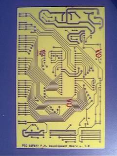
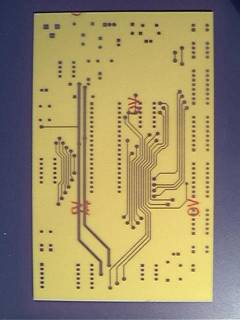
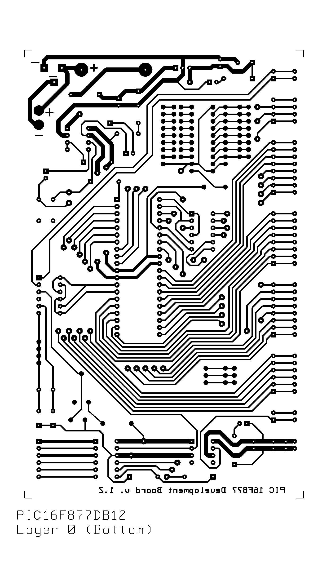
PCB layout printing In the images below you can see the circuit's layout and how to place components. If you haven't saved them yet, through the links in the beginning of this page, you can do it now. The images you can see below here are 100 or 300 dpi images. To obtain the same images, at 300 dpi, in a new window, from where you can print or save them, or simply watch them enlarged, you should just click on the images below or on the links under them, or, if you are using a Windows (TM) 95/98, you can use the right button and choose "Open link in new window". You can save just from this page the 300 dpi images on your hard disk or other media choosing "Save OBJECT with name" and print them later with your browser or other programs. With the browser you could have problems with the images' size, while, as an instance, Windows (TM) Imaging (TM) should print them in true size. If you are in doubt with regard to the size of the image you have printed, and you are in fear that it is not in true size, you can just measure the distance between holes for DIL components, which must be 2.54 mm between adjacent pins and 2.54 mm * 6 = 15.24 mm between the two rows of U1. Of course, not to make coarse mistakes, you could take as an example the distance between the first and the ninth pin, looking if it is 2.54 mm * (9-1) = 20.32 mm. You will not be able, of course, to measure hundredths of millimeters, and maybe not even tenths of millimeters (it would not be anyway very meaningful, given the size of pads and holes), but if your measure is a little bit more than 20 mm your printing should be good. To check the horizontal scale, you could measure as an example the distance between the two holes of a resistor; it must be 400 mils, that is 2.54 mm * 4 = 10.16 mm. If any of the two distances is not the one you are expecting, naming x that measure, you should apply a horizontal zoom factor of 10.16/x and a vertical zoom factor of 20.32/x. In the figure n. 4 you can see the components' placement with the board looked at from top and against the light. You can see there that the bottom side layout (soldering side), when exposing the board to the light for the photoetching, must be placed with the printed side in contact with copper. The images below are at low resolution, to save download time, but, as said, links allow access to higher resolution images. |
 |  |
| Fig. 1 - Copper side layout at 100 dpi | Fig. 2 - Components side layout at 100 dpi |
 | 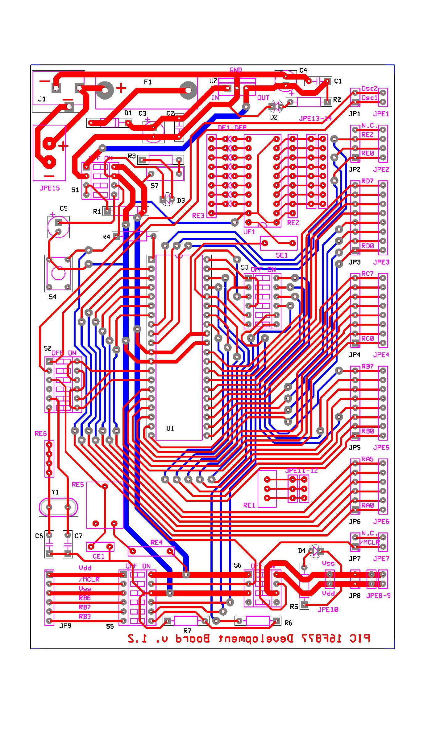 |
| Fig. 3 - Components placement on the board | Fig. 4 - Components placement and view of the bottom tracks (red, copper side) and top tracks (blue, component side) |
 |
| Fig. 5 - Electrical schematic at 100 dpi |
| Hoping I have been useful to you, just to me to wish you a good work! |
| Last update: 13 June 2003, 19.50 |