You are the visitor n.
Best view with 1024x768 |
You are the visitor n.
Best view with 1024x768 |
 |
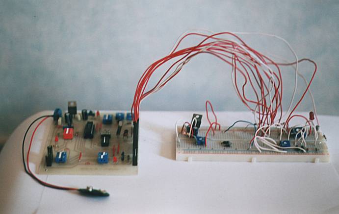 |
The F.F. Evaluation Board and connection to a prototype-board |
At the moment, sorry, the complete document is available in Italian version only. I am going to translate it as soon as possible. For your convenience, I have reported here the part still in Italian (the most part at the moment!); if you think you can find here something interesting, please bookmark this link and visit this page again. There is, of course, another possibility: "Learning Italian in thirty hours". It's not so difficult, why not trying? F. Iacopetti
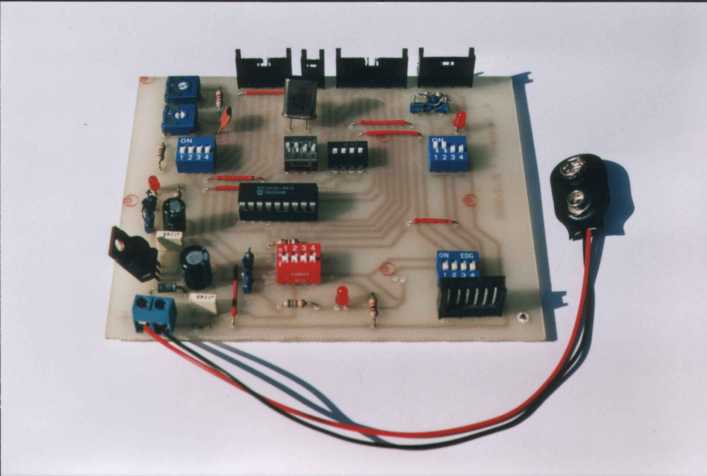
When I set, some time ago, about working with a PIC 16x84, I had immediately to face the problem to have a permanently and stably working circuit, without mounting the PIC on a prototype board every time. Searching on the net, I didn't find anything really complete for a PIC 16F84 / 16C84; I therefore decided to personally build an Evaluation Board allowing to operate with this microcontroller in the RC and XT modes, that is with a clock generated by resistor-capacitor net or by a crystal, but above all allowing to interface the PIC with external circuits in a very versatile and in the same time reliable way. So the Evaluation Board was born. I present here an improved version of it, which adds some functions to the original ones, but, how to say, I am attached to the first version. If you are interested in microcontrollers of higher families, you could take a look at the PIC 16F874 / 16F87 development board on this site. Disclaimers and acknowledgements This project is entirely personal, both in planning
and in realising; an acknowledgement goes to the software
allowing me to draw the printed circuit layout. The
program is PCB Elegance v 2.0 (I have the FREE 200 pins
limited version), realised by MERCO Electronics, which
has authorized me by e-mail also to non-personal
purposes. Attenzione: la versione della F.F. Evaluation Board presentata in questa pagina è la 3.0; si tratta di un circuito che è simile a quello della versione 2.0, riportata in fotografia, ma con alcune migliorie. La basetta visibile nell'immagine ospita un PIC 16F84 a 4 MHz, ma è compatibile anche con il PIC 16C84. Il circuito versione 2.0 è perfettamente funzionante sin dal Febbraio 2000 (from here the name F.F.), ma per mancanza di tempo sul nuovo circuito stampato i componenti non sono ancora stati montati. Anche se le modifiche sulla carta non dovrebbero incidere sulla possibilità di un corretto funzionamento, si tenga presente anche questa avvertenza. Indicheremo questa versione come "V. 3.0 Beta". Nel momento in cui anche la nuova versione sarà stata realizzata e collaudata provvederò all'aggiornamento di questa pagina. Note: Although it's theoretically possible to use other forms of supply, this Evaluation Board has been projected to receive supply from a 9V battery and interfaced only with circuits with low voltage batteries supply. In any case, be always aware of what you are doing! Being this material at free disposal of whoever
desires it, it is absolutely forbidden any form of use
for commercial purposes. |
Circuit's characteristics and description I
immediately say that this circuit is not a PIC
programmer, but it can be easily interfaced with one of
the many circuits of that kind that it is possible to
find, allowing this way the user not to remove the
microcontroller from the Evaluation Board while
programming it. Remark for switches and connectors' pins identification References to a particular switch belonging to the
dip-switch Sx will be made by Sx-n, where n and x are
integer numbers; the same convention for connectors JPx.
In particular, a reference to the switch Sx-1 points out
the first switch of the dip.switch Sx starting counting
from top in the design where all components, bridges and
tracks are reported; the same meaning when referring to
connectors JP. As an instance, you can see that S10-6 is
not connected to ny track; when opened, S4-4 is only
connected to S4-2 and to the PIC's pin n.15; when closed,
it is connected to JP2-2 and JP6-2, too. Let's now deal again with characteristics of the Evaluation Board. Supply: the circuit has been
projected for a 9V battery as a power supply, but it is
also possible to use an unregulated 7-15V DC source (a
7805 supplies 5V regulated to the PIC, possibly to a
programmer and also to an external circuit), or supply
from an external circuit through JP4 - S5 (please read
Microchip datasheets for suitable range). /MCLR pin: it is possible to
control it from an external circuit or by a programmer,
to connect it with a pull-up directly to Vdd, or even to
Vss through a capacitor so to realize a Power On circuit
(already present in the PIC); there is also the
possibility to reset the PIC by the S9 switch (not
viewable in the picture). Connection from and to external circuits
of Vdd, Vss, /MCLR: connection from or to
any external circuit of Vdd, Vss, /MCLR (this last one
whichever the power source is); connection of Vdd and Vss
from or to any programmer. Clock generation: 4 MHz
crystal, RC mode with two potentiometers for oscillation
around 1 MHz and 100 KHz; Possibility of programming the PIC
directly on the Evaluation Board: it is
possibile to connect the board to a programmer by a 5
wires connector, with the possibility to supply power to
the programmer or to receive power from it. Connection from and to external circuits
of I/O pins: all I/O pins are connected to
connectors to interface the PIC with an external circuit.
In the photos you can see only connectors for plugs,
while in the new version you can find both those ones and
SIL connectors for wiring. Spie alimentazione: tre led
inseribili singolarmente mediante jumpers indicano la
presenza di alimentazione in parti diverse del circuito e
ricordano di prestare attenzione ad evitare conflitti
elettrici fra le possibili sorgenti di alimentazione. Qualche applicazione |
Selection of working mode As previous said, the selection of working mode is realized by dip-switches. Let's describe their functions. |
Jumpers Quando chiuso, S7 permette al led D1 di indicare la presenza di tensione in uscita al 7805. S8 connette il led D2, il quale, in tal caso, indica la presenza di alimentazione al PIC, sia essa proveniente dal 7805, tramite S1, da JP9 tramite S10 o da JP4 tramite S5. S6 connette invece il led D3, il quale indica la presenza di tensione fra i piedini 1 e 3 del connettore JP4; tale tensione può ovviamente essere quella fornita dal circuito che alimenta il PIC (il 7805, tramite S1, o il programmatore, tramite JP9 e S10), con S5-1 e S5-3 chiusi, oppure provenire dal connettore JP4 (in tal caso essa raggiunge il PIC solo se S5-1 e S5-3 sono chiusi. |
Programmazione Per programmare il PIC senza rimuovelo dalla Evaluation Board, si devono innanzitutto collegare a JP9 opportuni segnali e tensioni provenienti dal programmatore. In dipendenza dal tipo di quest'ultimo, si deve adottare la giusta configurazione degli switch. If not otherwise specified, all switches must be put to OFF! In any case, be always aware of what you are doing! Pay a great attention to possible conflicts between feedings, and keep in mind that connecting together two wires of "common" (or ground, or earth) from different power supplies can provoke serious damage to circuits! Ad esempio, se alimentate il PIC e il programmatore con due diversi alimentatori, collegare fra loro i terminali "comune" (indispensabile) può essere molto pericoloso per la sopravvivenza dei circuiti stessi! Stessa cosa può succedere se state programmando il PIC con un programmatore collegato al computer e lo alimentate con un alimentatore! Attenzione! Quando avete dubbi, meglio utilizzare una batteria, la quale è flottante e si adegua al riferimento eventualmente imposto da un punto di connessione al circuito. Indipendentemente da quale sia il programmatore, consiglio vivamente, soprattutto nel caso il PIC sia collegato ad un circuito esterno mediante JP4, di scollegare i terminali RB6 e RB7 del PIC dal connettore JP3 ponendo su OFF S3-1 e S3-2. Consiglio inoltre di isolare i piedini Osc1 e Osc2 ponendo su OFF tutti gli switch di S2 e S4. I piedini RB6 e RB7 del PIC, naturalmente, devono essere collegati tramite S3-3 e S3-4 (ON) ai piedini S10-4 e S10-5, e da questi al programmatore collegato a JP9 ponendo su ON, appunto, gli switch S10-4 e S10-5. Siate inoltre sicuri che, nel caso sia il programmatore a fornire alimentazione al PIC, esso sia in grado di erogare una corrente sufficiente anche all'alimentazione del led D2 (circa 5 mA). 1) Programmer giving to the PIC feeding
(Vdd e Vss), /MCLR, RB6 and RB7. 2) Programmer receiving feeding (Vdd e
Vss) from the board. |
Components Note: all resistors are 1/4 W, 5%. R1, R8, R9 - 680 Ohm |
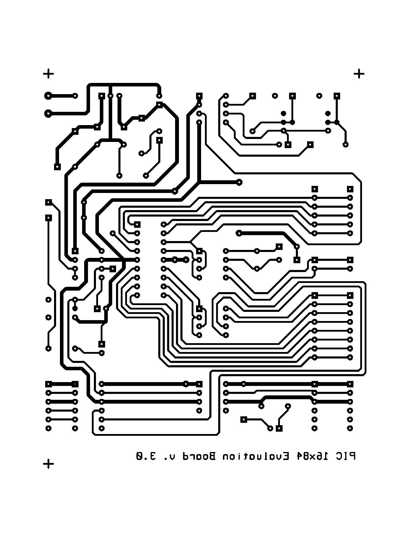
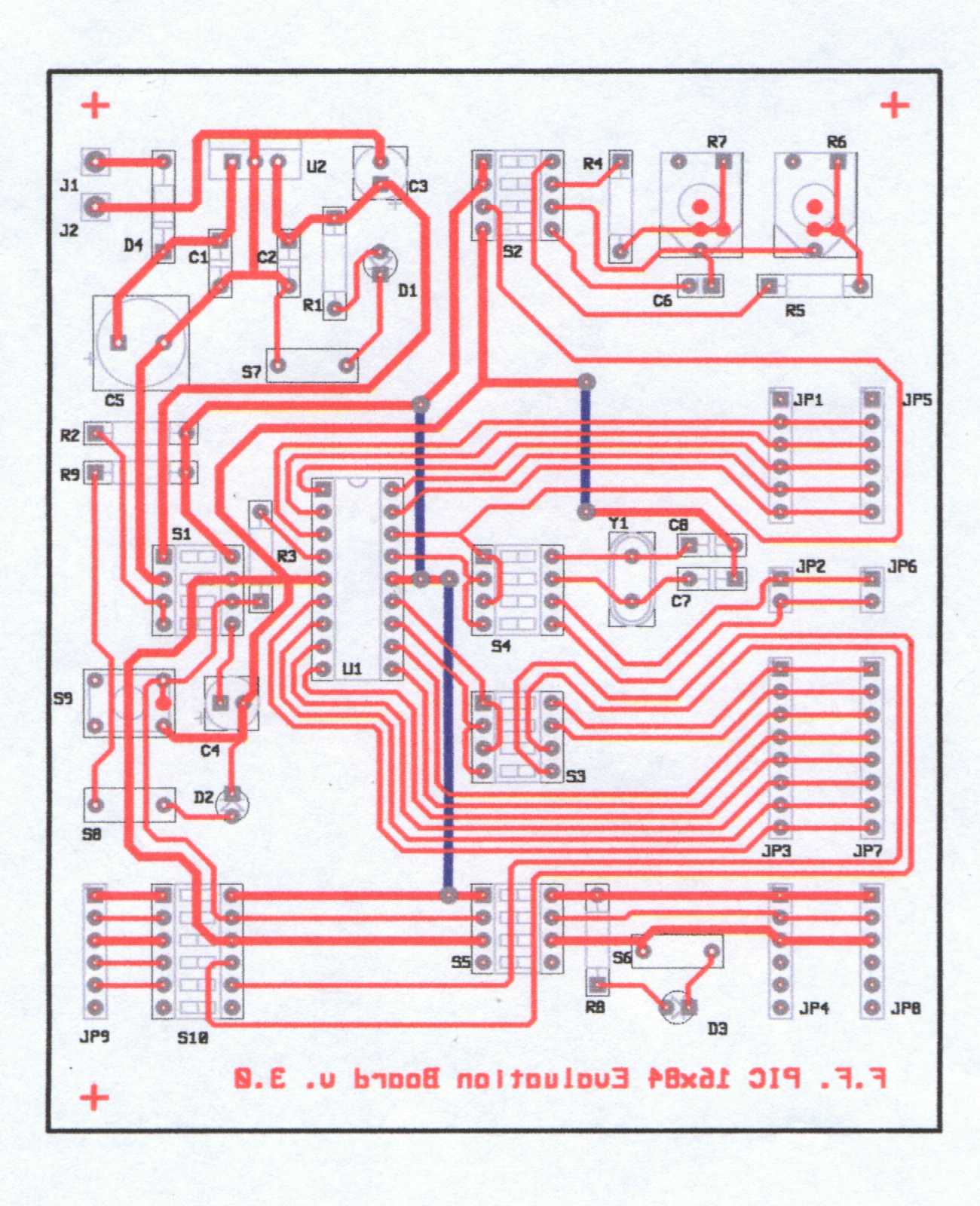
Realizzazione del circuito Sono riportate, nelle seguenti immagini, le figure relative al layout del circuito e alla disposizione dei componenti. Si tratta di immagini a 100 e 300 dpi. Per avere le immagini in una nuova finestra, da dove potrete stampare quelle a 300 dpi, potete fare click direttamente su quelle visibili qui sotto o sui link sottostanti, oppure, se utilizzate un sistema Windows (TM) 95/98, utilizzare il tasto destro del mouse e scegliere "Apri collegamento in un' altra finestra". In alternativa potete salvare le immagini sul vostro hard disk o altra memoria di massa con l'opzione contestuale "Salva immagine con nome" e stamparle in un secondo tempo con il browser o altri programmi. Con il browser si potrebbero avere problemi di dimensioni, mentre ad esempio Imaging (TM) di Windows (TM) dovrebbe stampare automaticamente con le dimensioni reali. Se avete dei dubbi sulle dimensioni della stampa ottenuta, perlomeno del layout lato rame, e temete che non sia a grandezza reale, provate a misurare le distanze fra i fori per i componenti DIL, che deve risultare di 2.54 mm fra piedini contigui e di 2.54 mm * 3 = 7.62 mm fra le due file. Ovviamente, per non incorrere in grossolani errori di misura, nel caso della distanza fra pin contigui utilizzate quella fra il primo e il nono piedino di una fila, assicurandovi che sia di 2.54 mm * (9-1) = 20.32 mm. Non riuscirete naturalmente ad apprezzare i centesimi di millimetro, e forse neppure i decimi (non avrebbe neppure senso viste le dimensioni finite delle piazzole e dei loro fori), ma se la vostra misura è appena superiore ai 20 mm dovreste essere a posto. La distanza fra le file dovrebbe invece essere approssimativamente appena superiore ai 7.5 mm. Se una delle due distanze non fosse quella attesa , detta x la relativa misura, dovreste applicare un fattore di zoom orizzontale pari a 7.62/x e un fattore di zoom verticale pari a 20.32/x. Nella seconda figura si nota la disposizione dei componenti con la basetta vista dall'alto e in trasparenza. Si notino i tre ponticelli (lato componenti) necessari al funzionamento del circuito. NOTE: the 300 dpi layout is suitable as a good quality master, as it has not the gray areas of the 100 dpi image. The schematic is visible in details in the 300 dpi version (257 KB). |
 |
 |
| The circuit layout at 100 dpi | Component placement and view of tracks and bridges (blue) |
 |
| Electrical schematic |
 |
| Component placement on the board |
| Hoping I have been useful to you, only to say: buon lavoro! |
| Last update: 28 Feb 2002, 23.47 | |